Next Generation Organic Substrate Technology: How Will it Synergize with 2.5D?
![]() Omar Bchir, Qualcomm Omar Bchir, Qualcomm
ABSTRACT: (to be added)
 Bio: Omar Bchir has worked in the field of IC packaging for 20 years. He joined Intel Corporation in 2004 as a Substrate Pathfinding Engineer. In 2008, he moved to Qualcomm, where he remained for eight years, forming a substrate team and eventually leading the Advanced Packaging team. In 2016, Omar joined Rockley Photonics, focusing on design and proof of concept for next-generation Opto-ASIC network switches for mega data centers. In 2017, he joined Micron Technology, focusing on memory packaging development and optimization for automotive customers. In 2020, Omar joined Amazon’s Project Kuiper, developing packages for terrestrial and space-based applications to support low-latency, high bandwidth satellite-based broadband internet access. Omar re-joined Qualcomm in 2023, and currently leads the Substrate and Module Systems Engineering Team. Omar received a B.S. degree in chemical engineering from the Georgia Institute of Technology, and a Ph.D. degree in chemical engineering from the University of Florida. He holds 42 issued U.S. patents and has authored 13 publications. Bio: Omar Bchir has worked in the field of IC packaging for 20 years. He joined Intel Corporation in 2004 as a Substrate Pathfinding Engineer. In 2008, he moved to Qualcomm, where he remained for eight years, forming a substrate team and eventually leading the Advanced Packaging team. In 2016, Omar joined Rockley Photonics, focusing on design and proof of concept for next-generation Opto-ASIC network switches for mega data centers. In 2017, he joined Micron Technology, focusing on memory packaging development and optimization for automotive customers. In 2020, Omar joined Amazon’s Project Kuiper, developing packages for terrestrial and space-based applications to support low-latency, high bandwidth satellite-based broadband internet access. Omar re-joined Qualcomm in 2023, and currently leads the Substrate and Module Systems Engineering Team. Omar received a B.S. degree in chemical engineering from the Georgia Institute of Technology, and a Ph.D. degree in chemical engineering from the University of Florida. He holds 42 issued U.S. patents and has authored 13 publications.
|
|
Advanced Photo-imageable Dielectric Film Enabling Sub-5-micron Patterning for Next-Generation Build-up Layer
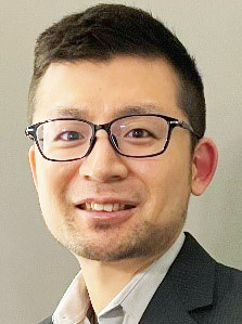 Hikaru Mizuno, JSR Micro Hikaru Mizuno, JSR Micro
ABSTRACT: As novel electronic products become dramatically smaller and more highly functionalized, semiconductor packaging structures are also required to become smaller, thinner and more complicated. Based on these market trends, the IC substrate has become one of the most important components in packaging. Next-generation build-up layer patterning materials for IC substrates are required to meet the demands of ultra-fine via patterning … (smaller than 5 micron) while also providing good thermomechanical properties such as a low coefficient of thermal expansion (CTE). In this presentation, we report our development approach and the performance of a novel photo imageable dielectric (PID) film material. The PID film shows a nearly vertical pattern profile with a sidewall taper angle of >85°, for 6 µm via features at 20 µm thickness. Small features of ?5 µm-via are also achievable at 10µm thickness. The thermal property of the PID film has a Tg of 260? and a CTE of 31 ppm/? after cure at 200?. Peel strength of plated Cu shows 0.38 N/mm for initial, and 0.46 N/mm after unbiased highly accelerated stress test (uHAST). Those properties meet typical requirements of a build-up material. It’s suggested that the novel PID film is a promising material for next generation build-up layers.
Bio: Hikaru Mizuno joined JSR Corporation in 2009 and worked in Fine Electronic Materials Research Laboratories. In 2018, he joined JSR Micro, Inc., and has been engaged in research and development of electronic materials especially RDL related materials. He has submitted 9 papers and 18 patents.
|
Dry-film Solder Resist Materials for high density IC Substrates
![]() Yuya Suzuki, Taiyo America Yuya Suzuki, Taiyo America
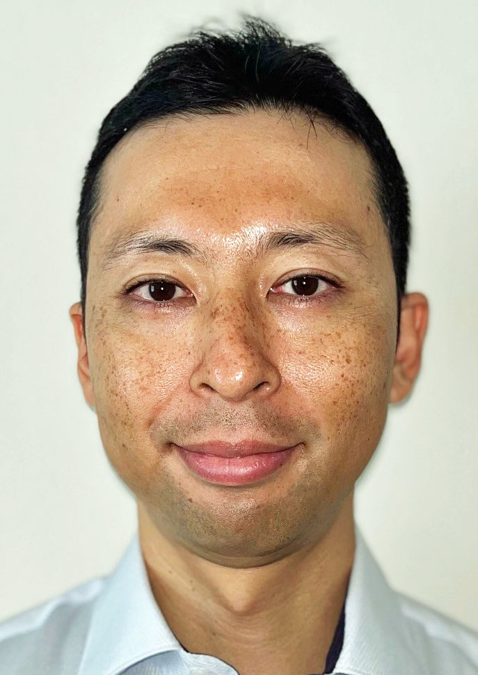 ABSTRACT: The demand for high-density integrated circuit (IC) substrates is driving advancements in material technologies to meet the increasing complexity and performance requirements of high-performance electronics. Solder resist (SR) materials play a critical role in IC substrate applications by providing insulation and protecting circuit patterns … from environmental and mechanical damage. Specifically, dry-film solder resist (DFSR) offers various benefits for advanced packaging, including refined thickness control, small-pitch opening capability, and excellent insulating reliability. These features enable DFSR to support precise electrical connections without signal interference while ensuring the integrity of fine-pitch designs. ABSTRACT: The demand for high-density integrated circuit (IC) substrates is driving advancements in material technologies to meet the increasing complexity and performance requirements of high-performance electronics. Solder resist (SR) materials play a critical role in IC substrate applications by providing insulation and protecting circuit patterns … from environmental and mechanical damage. Specifically, dry-film solder resist (DFSR) offers various benefits for advanced packaging, including refined thickness control, small-pitch opening capability, and excellent insulating reliability. These features enable DFSR to support precise electrical connections without signal interference while ensuring the integrity of fine-pitch designs.
This talk explores recent innovations in DFSR materials tailored for high-density IC substrate applications and examines material trends for next-generation technologies.
Bio: Dr. Yuya Suzuki is a technical marketing manager of Taiyo America. He has a Ph.D. degree in materials science from Georgia Tech, and has more than 15 years of experience in electronic materials for advanced IC packaging. Dr. Suzuki has published more than 30 papers in scientific journals and conferences.
|
|
Advanced Insulation Material for High Performance Semiconductor Packages
 Shiro Tatsumi, Ajinomoto Shiro Tatsumi, Ajinomoto
ABSTRACT: Printed circuit boards such as multi-layer printed wiring boards and flexible printed wiring boards are used for a wide variety of electronic devices. Ajinomoto Build-up Film®(ABF) has been widely utilized for a variety of package structures due to its outstanding insulation reliability, good resin flow, thickness uniformity and Semi-Additive Process (SAP) compatibility for fine line and space formation. Low coefficient of thermal expansion (CTE) and low transmission loss (Df) for high-speed applications are crucial for ABF qualities, in addition to the growing needs for larger packages. GL series were created as new ABFs for next-generation packages to satisfy these requirements.
Due to glass’s superior mechanical and electrical stability as well as its superior flatness, glass substrates have recently drawn the attention of package trends. These characteristics would help next-generation packages achieve lower energy consumption and higher density connectivity. Large packages with a high number of layers are also necessary for high performance computing applications to meet the demands of the rapidly expanding server and AI technologies. New ABF with low CTE (less than or equal to 17 ppm) and low Df (less than or equal to 0.003) was created to satisfy the requirements. minimal transmission loss is also a result of the new ABF’s minimal surface roughness, even after the desmear chemical etching procedure. These findings demonstrated that New ABF would meet the possible needs of upcoming package trends. Furthermore, nano-sized filler ABF (Nano filler ABF) was created to meet the high demands for ultra-thin layer to layer structure, small via, and fine line and space. To achieve the same performance as traditional ABF, nano filler ABF was developed with a maximum loaded silica filler size of less than 1 um. It helps create a smooth surface and an ultra-thin resin layer, which makes it possible to fabricate fine via, lines, and spaces. It was shown that employing the nano filler ABF, 2/2um line and space formation could be accomplished. Several techniques, including deep ultraviolet laser via, excimer laser via, plasma via, and Cu pillar, were used to study small via manufacturing. The latter, commonly known as the via-less technique, would need CMP following encapsulation with ABF, a nano filler. Using these via opening techniques, a via with a smooth via side wall shape and a diameter of less than 5 um was successfully opened. High density connectivity for FOWLP and FOPLP applications is made possible by these small via patterning techniques.
Bio: (to be supplied)
|
DGlass Compositions for Data Centers, AI, and Quantum Computing
![]() Vern Stygar, AGC Vern Stygar, AGC
 ABSTRACT: The use of glass as a core material for electronic and photonic packaging substrates is being considered due to its rigidity, flatness, and dimensional stability for advanced packaging such as chiplet packaging requiring large format and high-density interconnection. This presentation will provide an overview of glass material technology, processing technology and the need for reliability testing for glass core substrates. ABSTRACT: The use of glass as a core material for electronic and photonic packaging substrates is being considered due to its rigidity, flatness, and dimensional stability for advanced packaging such as chiplet packaging requiring large format and high-density interconnection. This presentation will provide an overview of glass material technology, processing technology and the need for reliability testing for glass core substrates.
Bio: Vern Stygar has worked in the semiconductor industry for more than 35 years and began his career as a process engineer at Beckman Instruments followed by 10 years at Ferro Corporation as the product manager for thick film paste and LTCC for high-frequency devices. In 2004 Vern joined AGC as the product manager for glass for semiconductor products. In his role as a product manager, Vern is responsible for advanced packaging for High Frequency products, co-packaged photonics and structured glass. Vern has authored or co-authored papers for high frequency applications utilizing glass, thick film and thin film metallization. Vern holds a degree in Chemistry and an MBA.
|
|
Substrate Materials for Advanced Packaging
 Masa Fukui, Resonac America, Inc. Masa Fukui, Resonac America, Inc.
ABSTRACT: The development of advanced packaging technology has been accelerated, such as for 2.5D packaging and chiplet design. Advanced packaging requires HSIO, high density interconnection and large form factor. This motivation for future packaging is the driving force behind the development of substrate materials to meet the challenges. In this perspective, glass substrates are considered as the future generation substrate, while at the same time, the development of glass-like organic substrates is accelerating. Substrate materials with superior physical properties can be made thinner while maintaining low warpage, thereby enabling fine pitch through-hole and reducing signal loss. Coplanarity, dimensional stability and small thickness variation are required to improve manufacturing yields for large-size packages. The latest development status and technical direction for organic substrate materials will be presented.
Bio: Masa Fukui (to be provided)
|

 Bio: Omar Bchir has worked in the field of IC packaging for 20 years. He joined Intel Corporation in 2004 as a Substrate Pathfinding Engineer. In 2008, he moved to Qualcomm, where he remained for eight years, forming a substrate team and eventually leading the Advanced Packaging team. In 2016, Omar joined Rockley Photonics, focusing on design and proof of concept for next-generation Opto-ASIC network switches for mega data centers. In 2017, he joined Micron Technology, focusing on memory packaging development and optimization for automotive customers. In 2020, Omar joined Amazon’s Project Kuiper, developing packages for terrestrial and space-based applications to support low-latency, high bandwidth satellite-based broadband internet access. Omar re-joined Qualcomm in 2023, and currently leads the Substrate and Module Systems Engineering Team. Omar received a B.S. degree in chemical engineering from the Georgia Institute of Technology, and a Ph.D. degree in chemical engineering from the University of Florida. He holds 42 issued U.S. patents and has authored 13 publications.
 Hikaru Mizuno, JSR Micro
 Shiro Tatsumi, Ajinomoto