Mini-Colloquim on Advanced Packaging and Heterogeneous Integration
Pizza lunch with two technical speakers.
Date and Time
Location
Hosts
Registration
- Date: 18 Feb 2025
- Time: 12:00 PM to 03:00 PM
- All times are (UTC-05:00) Eastern Time (US & Canada)
-
 Add Event to Calendar
- 257 Fuller Rd
- Albany, New York
- United States
- Building: Nanofab South
- Room Number: NFS Auditorium
- Starts 03 February 2025 12:00 AM
- Ends 18 February 2025 05:00 PM
- All times are (UTC-05:00) Eastern Time (US & Canada)
- No Admission Charge
Speakers
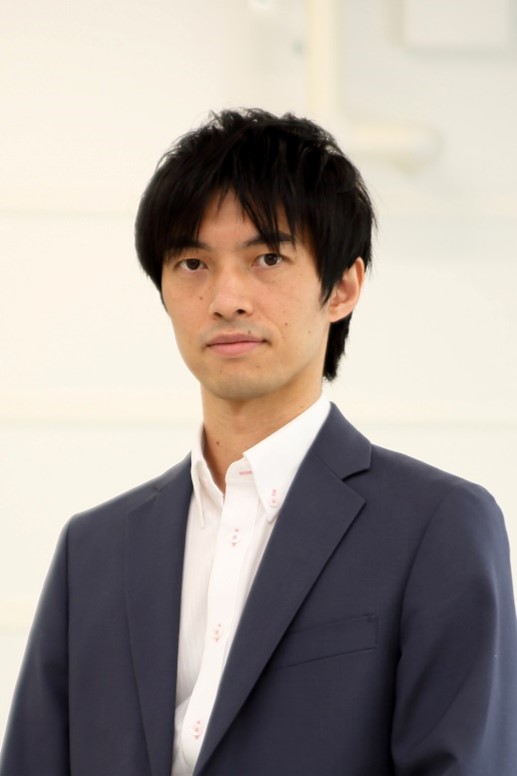
Fumihiro Inoue
Key Technologies and Mechanism Analysis for Next-Generation Hybrid/Fusion Bonding
Despite its growing importance for wide range of applications and architectures, the mechanisms underlying “bonding” remain inadequately understood. SiCN is a promising candidate as a wafer bonding dielectric film due to its high bonding quality and reliability, even under low thermal budgets, whereas SiO2 remains the conventional choice. In recent years, there has been a surge in reports on SiCN's adoption for bonding applications. As its use advances, investigating the mechanisms of SiCN bonding has become essential to optimizing bonding process conditions. Additionally, achieving ultimate distortion control is critical for precise overlay corrections during lithography. Bond wave behavior, the primary contributor to wafer bonding distortion, remains insufficiently explored. Plasma activation and surface wetting are thought to strongly influence bond wave speed, yet their surface-level interactions are poorly understood. Furthermore, the lack of standardized bond strength measurement methods introduces significant variability in results.
Die-level hybrid bonding is a key integration technology for future AI architectures with 3D chiplet. However, challenges such as the lack of standardized bond strength measurement methods and limited understanding of Q-time for die-level bonding have caused delays in the implementation of direct placement for die-to-wafer bonding.
In this presentation, we will share our latest findings on the comprehensive study of wafer/die bonding mechanisms. These insights aim to support the evolution of future node 3D architectures
Biography:
Fumihiro Inoue is an Associate Professor at Yokohama National University, specializing in 3D integration and chiplet. Before joining the university, he contributed extensively to advancing unit processes for 3D integration during his role as researcher at imec, which lasted until 2021. In recognition of his significant contributions to the field, he received the prestigious IEEE EPS Outstanding Young Engineer Award in 2022. Since April 2024, Dr. Inoue has also served as the Vice-Director of the Semiconductor and Quantum Integrated Electronics Research Center at Yokohama National University, where he continues to lead cutting-edge research initiatives
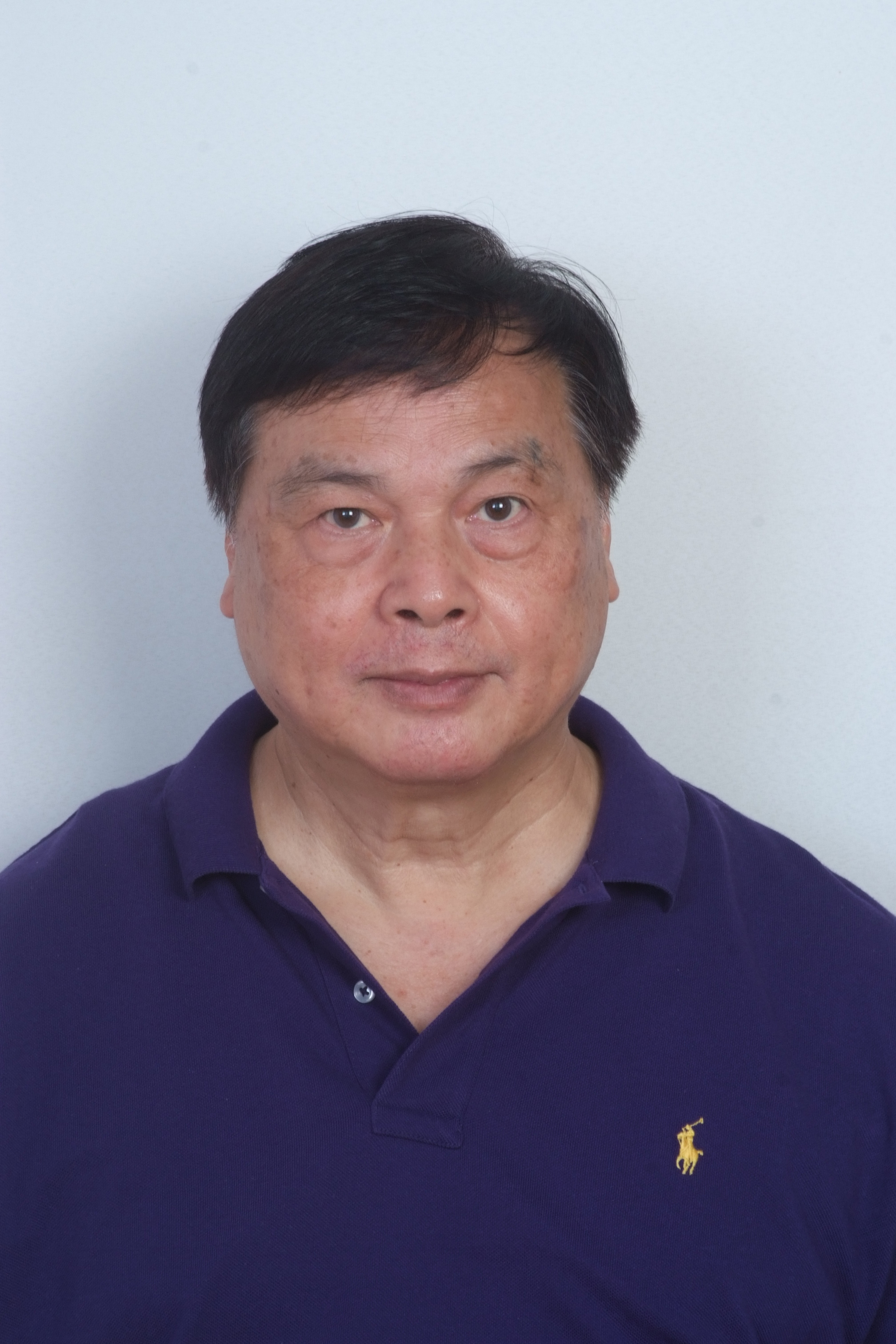
John Lau
Advanced Substrates for Chiplets and Heterogeneous Integration
Advanced Substrates for Chiplets and Heterogeneous Integration
Biography:
John H Lau, with more than 40 years of R&D and manufacturing experience in semiconductor packaging has published more than 535 peer-reviewed papers (375 are the principal investigator), 51 issued and pending US patents (35 are the principal inventor), and 23 textbooks (all are the first author). John is an elected IEEE fellow, IMAPS Fellow, and ASME Fellow and has been actively participating in industry/academy/society meetings/conferences to contribute, learn, and share.
Agenda
12-1 pm Pizza Lunch
1-1:10 pm Welcome / EPS Overview
1:10-1:55 pm John Lau, Unimicron Technologies
1:55-2:00 pm Break
2:00-2:45 pm Prof. Inoue, Yokohama National University
2:45-2:55 pm Closing comments